Research at Molecular and Nanoelectronics Research Group (MNRG)
Department of Electrical Engineering, Indian Institute of Technology Indore, Madhya Pradesh.
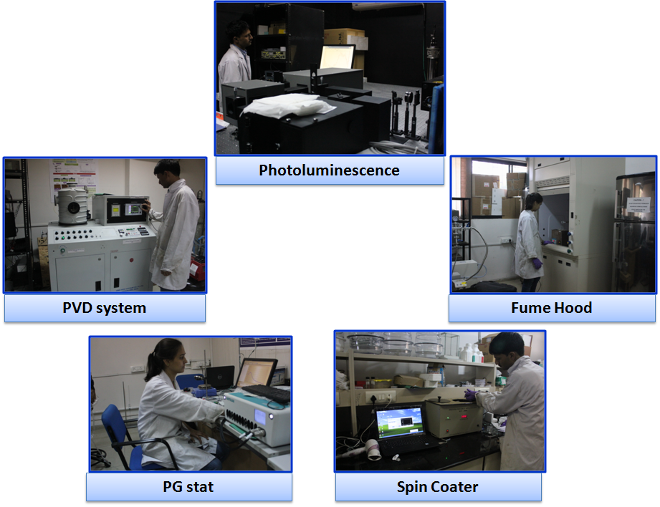
Members of MNRG are actively engaged in the theoretical study as well as fabrication and characterization of discreet electronic devices, with an overall aim towards improvisation of their performances. Our interest ranges from organic to some of the inorganic materials. We are mainly focussing towards development of cheap alternatives for mass scale fabrication of electronic devices. One of the main target of our group is directing our efforts towards fabrication processes that are essentially soft and wet. At the moment our research activities include efforts towards the development of thin film transistors, Light Emitting Diodes (LEDs), Photovoltaic Devices, Photodidoes and Biosensors. In order to achieve this aim we have several important fabrication/characterization equipments with us as listed below
-
Physical Vapor Deposition (PVD) System based on resistive heating approach for coating metal electrodes.
-
Photoluminescence Spectroscopy for studying emission emanating from thin films and solutions.
-
IV measurement system (Keithley 2612) for measuring current voltage characteristics of two and three terminal devices.
-
LCR meter (Hioki 3532) for measurement of inductance, capacitance and resistance and various other frequency dependent parameters.
-
Spin Coater for coating thin films cast out of solutions.
-
Potentiostat/Galvanostat (Autolab) for carrying out various electrochemical measurements viz. amperometric, potentiometric, conductimetric and chronoamperometric as well as cyclic voltammetry etc.
-
Hall measurement system, for measuring 4 probe conductivity etc.
-
Oven for annealing freshly prepared samples.
-
Ultrasonicator bath for cleaning of samples.
-
hot plate with stirrer for preparation of solutions.
-
Grade one millipore deionised water system.
-
Fumehood.
Project(s)
-
DST Fast Track Project titled, "Development of High Sensitivity Organic Photo Transistors Through Fine Control of Film Morphology and Interfacial Effects", Budget: 24 Lakhs
Summary of Post Doctoral Research Work (April 2009- November 2010)
Nanosystems Integration Laboratory, Research Institute of Electronics, Shizuoka University.
Group leader:- Prof. Hiroshi Inokawa (view staff members here)
Since the early discovery tunneling of single electron and Coulomb Blockade phenomena in the 1980s, it was envisioned by the scientists worldwide that if the size of the quantum dots is reduced to several nanometers, it is highly possible to produce single electron transistor (SET) that works above liquid nitrogen temperature, and thus will bring the revolution in the VLSI industry. Since then SET has been a hot area of research. The breakthroughs in nanotech and their combination with the already established state of the art VLSI industry gives a lot of hope to SET.
Usually electrons move continuously in common MOS Transistors. However, as the size of the system goes down to nanoscale, the energy of the system becomes quantized, that is, the process of charging and discharging becomes discontinuous. The energy for one electron to move into the system is Ec = e^2/2C. Where C denotes the capacitance of the system. This Ec is called Coulomb Blockade energy, which is the repelling energy of the previous electron to the next electron. This energy can be considerably high for a tiny system, as a QD. Thus the electrons in such a system cannot move simultaneously, but pass through one by one. If two QDs are joined at a point and form a channel, it is possible for an electron to pass from one dot over the energy barrier to move over to the other dot, this phenomenon is called quantum mechanical tunneling. In order to overcome the energy barrier Ec, the applied voltage on the quantum dots (V/2) should be V > e/C. In order to observe Coulomb Blockade and tunneling the energy that an electron assumes must be higher than the scattering thermal energy, i.e. e^2/2C > kT. (Where k denotes Boltzmann constant).
This equation clearly shows that if the capacitance is low enough, and if the size of QDs can be reduced to several nm, Coulomb blockade and tunneling can be observed at room temperature (RT) as well. In general an SET consist of two tunnel junctions which are connected by a Coulomb island, whose potential can be controlled by the gate capacitance Cg. A voltage Vg applied to the gate controls the opening and closing of the SET as shown in the Figure below. Rs and Cs and Rd and Cd denote the resistances and capacitances of the two tunneling junctions respectively.
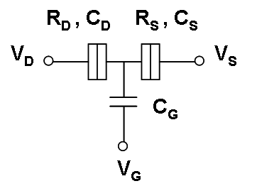
It is due to this unique structure that SET has many prospective potential applications, viz. Low power consumption circuits, high sensitivity, high switching speed, high packet density, etc. Also, It is due to these, that SET has attracted considerable attention towards its fabrication and industrial realization.

Summary of PhD Thesis
Kaneto Laboratory, Graduate School of LSSE, Kyushu Institute of Technology, Kitakyushu Science and Research Park, Japan.
Research Guide: Prof. Keiichi Kaneto
In the recent past, conjugated polymer based electronic devices viz. Polymeric Solar Cells (PSCs), Polymeric Light Emitting Diodes (PLEDs) and Polymeric Field Effect Transistors (PFETs) have gained special interest due to their transport properties as well as their potential application for the development of cheap and flexible electronic devices. It has been observed that the interface between various polymeric layers and also between polymer and metal is very crucial for development of high performance devices. It is widely accepted that coating a thin layer (< 2nm) of LiF below Aluminum (Al) leads to improvement in the charge injection from the cathode into the LUMO of n-type organic semiconductor, and leads to improvement in the efficiency of PLEDs. Similar improvement in the quantum efficiency of thin film bulk heterojunction (P3HT/PCBM) PSCs has also been observed. Although several models have been proposed to explain this effect, however, still there exists an ambiguity whether LiF dissociates into ions and thus causes doping of the semiconductor layer immediately below it, or does it create a vacuum level offset between the semiconductor and cathode.
In this regard a comparative study was performed between the Al(2nm)/Poly(3- Hexylthiophene)(P3HT) junction and LiF(2nm)/P3HT junction. It was demonstrated that LiF does not form a depletion layer with P3HT by a combined study of Photoluminescence (PL) and Photo induced memory devices (PIMDs). This fact was then utilized to cut-off the bulk region in a P3HT based Organic Field Effect Transistors (OFETs) to improve the on/off ratio in these devices. Further, It was observed that metal coating on the conducting polymer led to the increase in high energy peak in the PL emission spectra. It was later attributed to the increase in the intrachain disorder due to 30nm thick coating of Al on top of P3HT film.
A unique model to study the depletion layer optoelectronically using bias dependent PL spectra was developed, and later demostrated experimentally. Using this model the non uniform distribution of charge carriers in the bulk of P3HT was demonstrated. Later this model was used to study the Al/P3HT and Al:LiF/P3HT junctions to further elucidate the effect of LiF in bilayer structures, which is in particular significant for the development of PSCs. It was found that in bilayered structures LiF helps in creating high electric field over a narrow region of its interface and hence leads to better dissociation of excitons near the interface that further leads to improved quantum efficiency of PSCs. Moreover, it was also observed that inclusion of LiF also protects the pristine polymer film from the hot Al atoms during the thermal deposition process.
This optoelectronic technique was further successfully applied to various other organic materials to investigate the role of morphology in the field assisted dissociation of excitons. In order to change the morphology a series of Poly (3-Alkylthiophene) PAT films were studied. These PAT films differed in their regioregularity as well as the length of their alkyl chain substituent. It was found that better film morphology ensures easy diffusion of excitons formed in the bulk of semiconductor, to the interface and hence leads to better field assisted dissociation of excitons. Thus our technique can also be used to probe different materials for their possible photovoltaic applications. In the end the bias dependent PL spectra under the forward bias regime for ITO/P3HT/Al Schottky cell was studied, and clearly gave the evidence of PL quenching caused by injected charge carrier in the P3HT film. It was observed that the space charge built up in the bulk of P3HT causes change in morphology of the film and thus leads to the observed PL quenching.
(get my PhD thesis here)
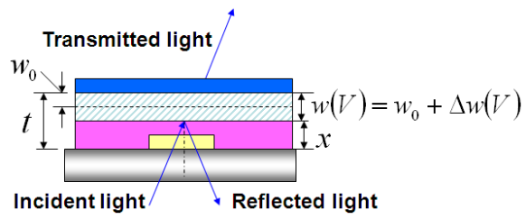
Fig.1 Shows the concept of basic principle of operation of bias dependent Photoluminescence.
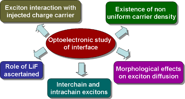
Fig. 2 Shows the Interrelationship between the optoelectronic study of interface and various related effects that I have observed in Polymer based thin film devices.
Other Links